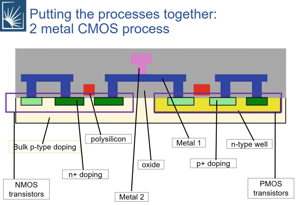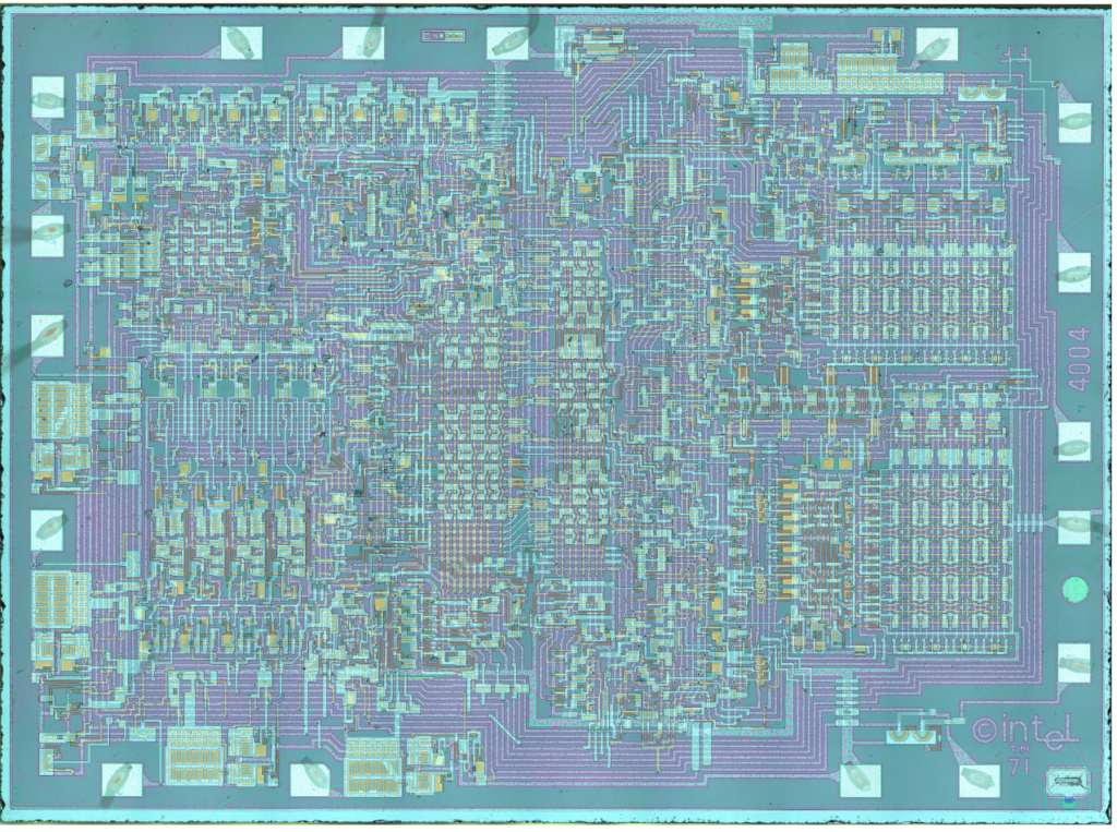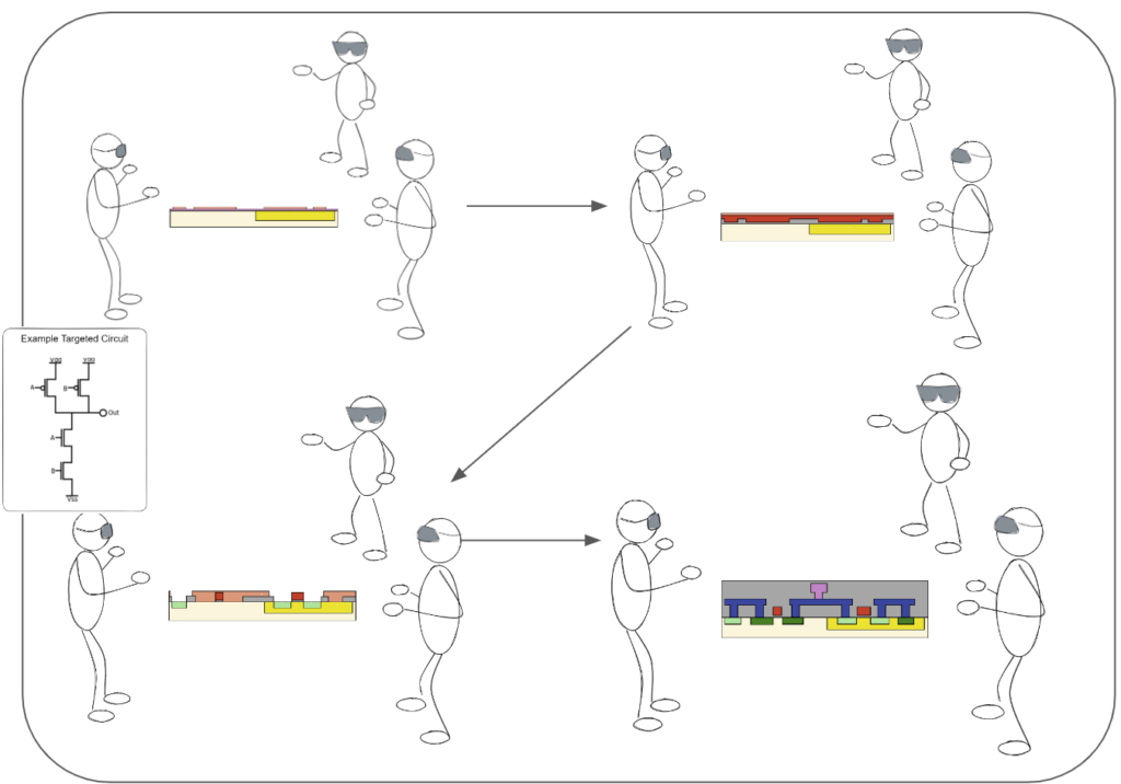
Dr. Allison Hess-Dunning teaches about the fabrication of the tiniest devices, such as semiconductors. The process is a complicated recipe of layering on and peeling off certain elements that either conduct or inhibit conduction, and the precise patterns determine the device’s functionality. 2D circuit maps and cross-sections are typically used to describe process flows, however they can be difficult to follow especially for students relatively new to the field.
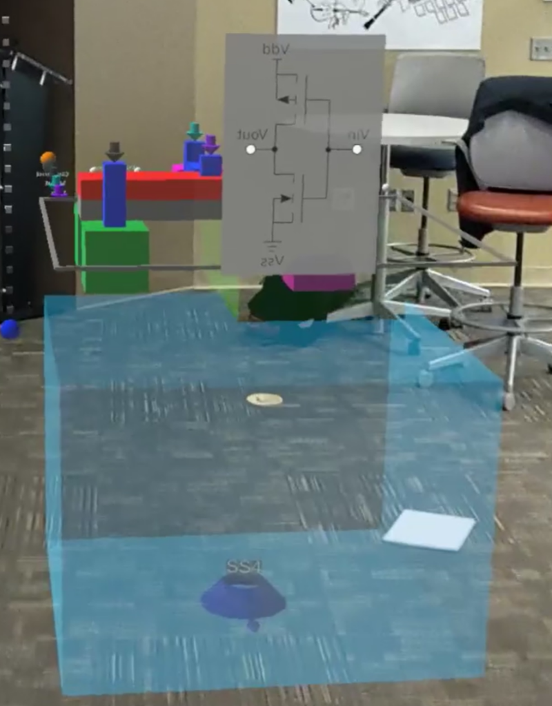
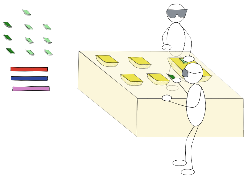
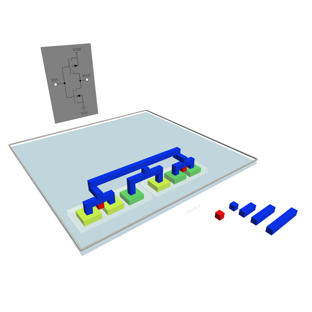
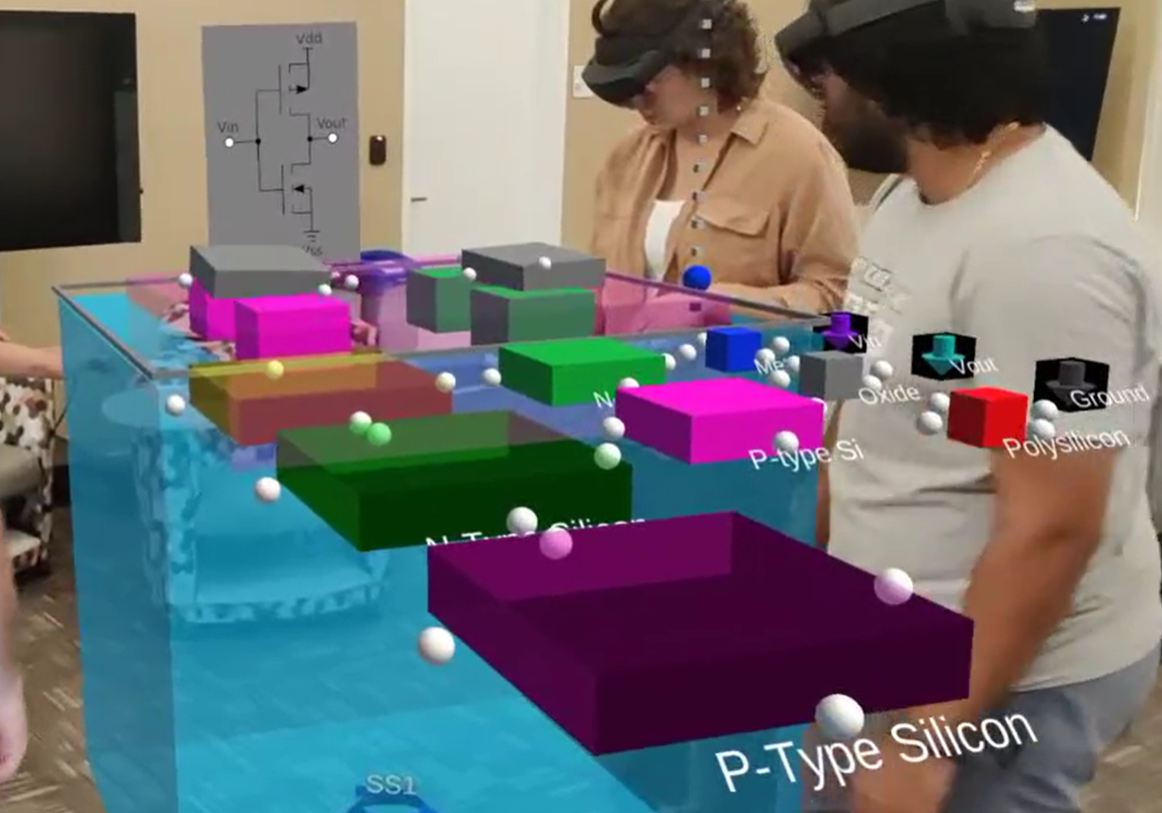
In the app developed during her fellowship year (SolidState), users are presented with a holographic bulk silicone substrate base and a repository of typical semiconductor parts (e.g., n-type and p-type wells.) Following a provided targeted circuit map, students build the semiconductor by adding in parts at various levels and locations. Eventually, Dr. Hess-Dunning imagines adding additional types of transistor devices and MEMS (Micro Electro-Mechanical Systems) and adding simulated current flow to test functionality.
